


Surface temperature monitoring during contour laser welding of plastics
17. 12. 2019
Flare monitoring: Thermal imaging monitoring of burning and fires starting in chimneys
17. 12. 2019While the design and production of printed circuit boards (PCB) is a highly delicate process, it is very difficult to discover manufacturing defects or design imperfections in circuit boards. Traditional optical inspection methods are often insufficient for the identification of major faults. However, alternative inspection methods are available.
When a PCB is supplied with voltage, electric current flows through the board, which starts to heat up. PCB thermal fields can then be determined and visualized by thermal imaging via a thermal camera. With sufficient knowledge of the thermal field, manufacturing defects can be discovered early in the design process. Thermal imaging can also be effective during series or prototype manufacturing.
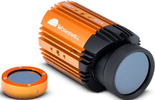
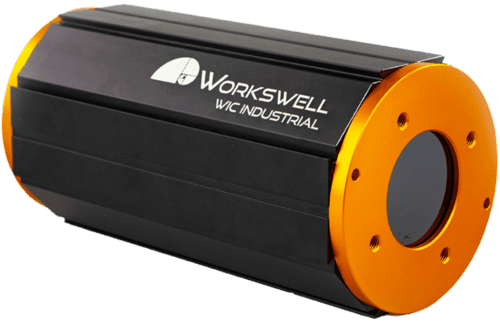
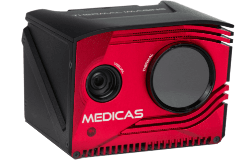
In the PCB design stage, thermography can be used to visualize the excessive heating of certain components. This can be caused by a range of defects, which include electric short circuits, incorrectly mounted components, and insufficient tin during soldering. These problems can be resolved with the application of a Workswell WIC thermal camera.

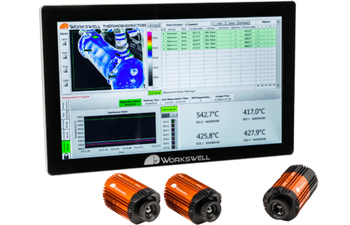
Thermal imaging has an important role to play in the simultaneous inspection of a large amount of mounted PCBs, and it also can facilitate the immediate discovery of a wide range of issues after PCBs are mounted. If, for example, a component is incorrectly mounted and there are cold joints, components may undergo significant heating. In the first phase of traditional equipment testing, these sorts of defects will often slip by undetected. However, during longer operation, components may stop functioning because of high temperatures, and the entire board may stop working. These problems can be discovered with a Workswell WIC thermal camera immediately after PCB mounting and activation without any need for functional testing. An operator will discover any deviation from the norm by comparing the thermal images of a functional PCB with the tested PCB, even if they have no knowledge of PCB design.
Thermal imaging enhances the PCB design process, and it can even shorten PCB development time. If the layout design is incorrect, a high current will flow through some parts of the PCB and produce excessive heat. This will in turn make the PCB unstable and shorten its service life. Yet these design problems are very difficult to discover without a thermal camera.
With a thermal camera, on the other hand, designers can ascertain the overall allocation of heat and add coolers and other components accordingly. For example, when compiling the code for an FPGA, chip routing may be less than optimal. A thermal camera is the ideal tool for the discovery of these issues because an imager with the sensitivity of the Workswell WIC can detect excessive loads on some parts of the greater chip.

